Welcome To Laminar Enterprise
Professional In Printed Circuit Board(PCB)
Trading and Distributor of Electrical & Solder Wire Products.

The PCB Market Story
Welcome to Laminar Enterprise which is Located in Jogeshwari (East), Mumbai , India. Our business goal is to be the most professional PCB.
We became pioneers in the development and manufacturer of led mounted PCB. Laminar Enterprise is one stop solution for all your requirements starting from PCB layout to PCB assembly, Stencil fabrication. Hire us for your required services and keep all your worries at back burner because you are at the best place.
Today, PCB Market is known across the market as one of the pioneers who have brought global standards to Indian markets.With customer-centricity at its core, innovation in its DNA, extensive investments in human capital, and an intricate focus on excellence across all its touchpoints, PCB Market has evolved into a value-augmenting platform for the entire electronics ecosystem. With customer-centricity at its core, innovation in its DNA, extensive investments in human capital, and an intricate focus on excellence across all its touchpoints, PCB Market has evolved into a value-augmenting platform for the entire electronics ecosystem.
Industries We Serves
Powerful Features of Proven Expertise In Industrial Partnerships.
Our Services
Specialized High Precision Printed Circuit Boards.

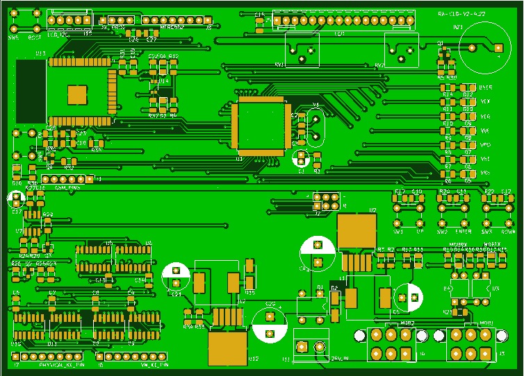
PCB Layout
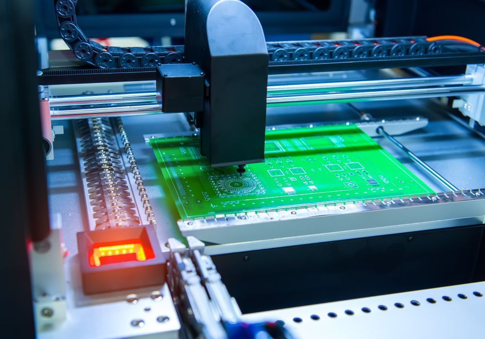
PCB Assembly
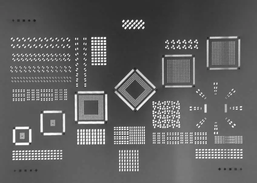
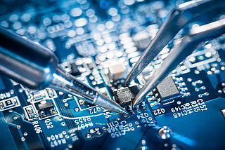
Stencil Fabrication
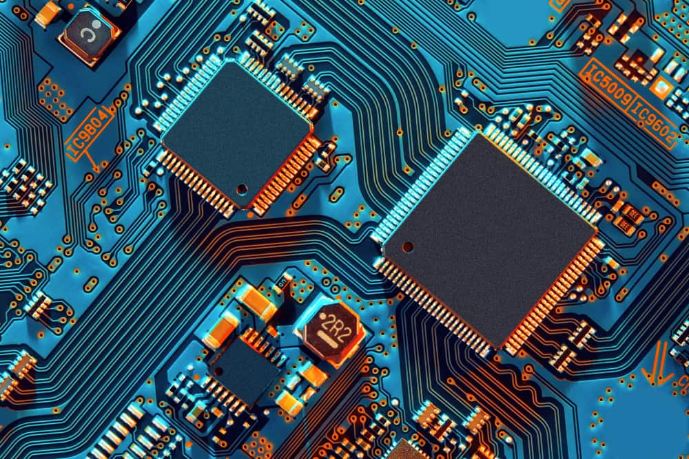
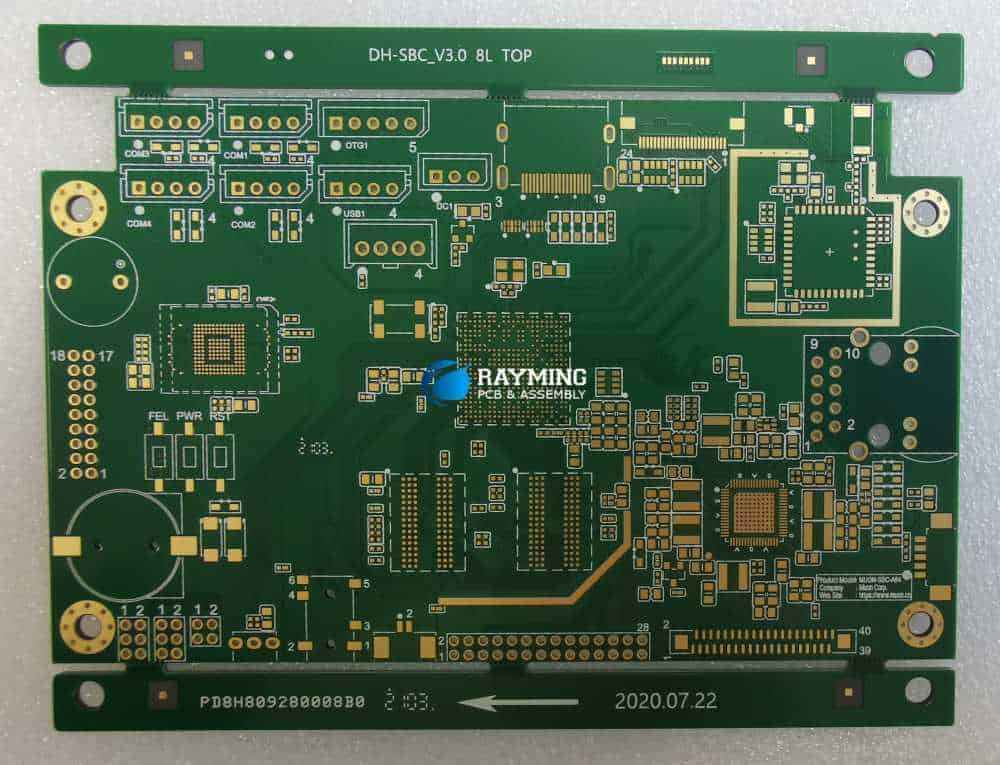
PCB Fabrication
Equipments
Capability
- Drilling.
- Routing
- MLB press
- Plating
- Finishing
- Photo Imaging
- Quality & inspection
- Flying probe testing machine.
Standard
- Excellon cnc 4 ( 3 spindle ) minimum drill dia 0.4 mm
- Posalux
- Hydruallic USA 3 day light hot press
- Full deasmer electroless PTH line.
- 600 x 450 mm
- 7 Mil
- 0.05 mm
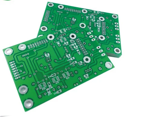
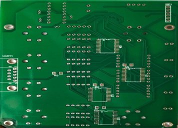
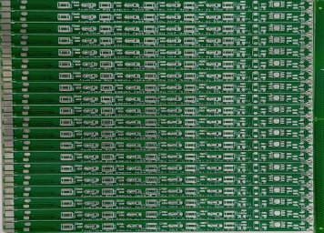
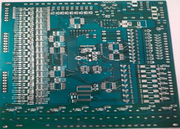
Our Products
Laminar Enterprise tries their best to provide high quality PCB Products.
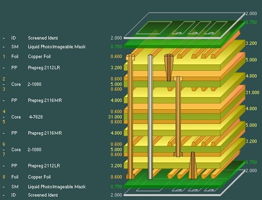
Multilayer PCB
There is a increased demand for products using the Multilayer PCB.To reduce size of product & for betterfunctionality which depends on the interconnection between the layers that it is made up of. Without microvia production improvements, PCB manufacturers are forced to increase product size to improve performance. The increasing cost of property is driving all industries to seek smaller products, lowering the demand for end products that contain thick, high-layer count printed circuit boards.
- Layer 1 : Device and signal1.
- Layer 2 : Power plane.
- Layer 3 : GND plane.
- Layer 4 : Signal 2.
- Layer 5 : GND plane.
- Layer 6 : Signal 3.
- Layer 7 : Signal 4
- Layer 8 : GND plane
- Layer 9 : Signal 5
- Layer 10 : GND plane
- Layer 11 : Power plane
- Layer 12 : Devices and signal 6
Blind & Burried PCB
The demand for faster processing times and reduction in size continues to drive the need for increased layer-count in printed circuit boards. One of the results of these design and technology requirements is the need for blind and buried vias. Incorporating blind or buried vias into a multilayer circuit board demands a higher level of innovation in PCB development. To manufacture these types of vias in a multilayer PCB requires either a process of sequential lamination of prepared components, or precise drilling of a completed multilayer PCB. Both methods demand additional time and attention in engineering and manufacturing to produce as compared with lower technology PCBs. Utilizing vias in your multilayer PCBs can significantly increase the number of connections without increasing the size. This brings speed and power to your project without compromise.
Double Sided PTH PCB
The double sided PTH PCB is the universal workhorse of the electronics industry. The complexity and density of components means much equipment has to use both sides of the Printed Circuit Board - and better products usually supplement this with plated-through-holes where the copper connections go right through the connecting holes to the opposite side of the board. These all the way through the board connections make double sided PTH PCB a much more physically robust item.
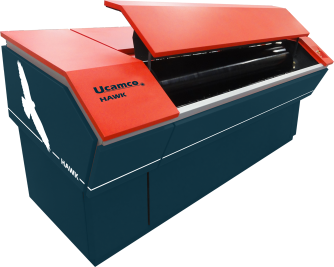
Laser Photoplotting
Technical Specification
Capability
- Mechanism.
- Addressability.
- Accuracy
- Repeatability
- Max Image Size
- Film Thickness
- Minimum Trace width
Standard
- Laser photoplotting.
- 4000 DPI
- +/- 0.05 Mil.
- +/- 0.1 Mil
- 600 x 450 mm
- 7 Mil
- 0.05 mm
Single Sided PCB
A single-sided PCB is a type of PCB where the components and conductive copper are mounted on one side and the conductive wiring is on the other side. Single-sided PCBs are the first-ever printed circuit board technology and are widely used due to their simplicity in manufacturing.
Metal Core PCB
A Metal Core Printed Circuit Board (MCPCB), also known as a thermal PCB or metal backed PCB, is a type of PCB that has a metal material as its base for the heat spreader portion of the board.
The analysis showed that PCBs consist of approximately 26% metal, made up mainly of copper, lead, aluminum, iron and tin, as well as other heavy metals such as cadmium and nickel
Why Choose Us
Quality, Service, Reliability
We measure the value we have created, by the degree of efficiency and effectiveness our customers attain with our services.
- 15+ Years of Expertise.
- Comprehensive PCB Solutions in One Place.
- Quality You Seek, Without Quantity Restrictions.
Manufacturing and Technical Questions
Contact Us
Get in touch
Location :
Unit No.205, Rolex Heights, next to Mepal Plaza, A-Wing, Subhash Road, Jogeshwari East, Mumbai, Maharashtra 400060
Email :
laminar.entp@gmail.comCall :
Navin Shetty(CEO) : 9324403605
Prakash Khandare (Marketing Executive): 9920841348
Rajesh Thakur(Marketing Executive): 9820778933